There is no such thing as a standard printed circuit board. Each PCB has a unique function for a particular product. Therefore, producing a PCB is a complex, multi-stage process. This overview covers the most important steps when producing a multilayer PCB.
When you order PCBs from TCX, you are buying quality that pays for itself over time. This is guaranteed through product specifications and quality controls that are far more stringent than those of other suppliers, and ensures that the product delivers what it promises. The production flow chart below illustrates ways the TCX process is unique or goes beyond the IPC standard.
If you cannot find the answer you are looking for, or would like more details, then please contact us and we would be more than happy to assist.
Customer supplied data (Gerber) is used to produce the manufacturing data for the specific PCB (artworks for imaging processes and drill data for drilling programs). Engineers compare demands/specifications against capabilities to ensure compliance and also determine the process steps and associated checks. No changes are allowed without customers' permission.
TCX ADDED VALUE With 10+ evaluated and approved pre-production engineers handling your data, TCX builds in security from the very start of the process.
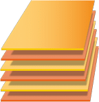
Material of various types are received from approved sources and held in controlled environments until required. Specific material is released into production for a specific purchase order with base materials cut to the required sizes. All materials used can be traced back to their manufacturing batch.
TCX ADDED VALUE
materials – In addition to customer-specified materials, TCX only uses internationally renowned materials.

Stage 1 is to transfer the image using an artwork film to the board surface. The traditional method is using photosensitive dry-film and UV light, which will polymerise the dry film exposed by the artwork. Another more advanced method is to use an LDI exposure machine, which has high resolution and can automatically adjust the compensation coefficient according to the expansion and contraction of the PCB. This step of the process is performed in a clean room.
TCX ADDED VALUE
TCX use an LDI exposure machines for high pression circuit boards.
The control standard of the clean room is 100,000 grades.

Stage 2 is to remove the unwanted copper from the panel using etching. Once this copper has been removed, the remaining dry film is then removed leaving behind the copper circuitry that matches the design.
TCX ADDED VALUE
Using DES (Develop, etch, and stripping) production line to reduce quality issues like scratches, foreign material, etc., and improve production efficiency.
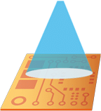
Inspection of the circuitry against digital “images” to verify that the circuitry matches the design and that it is free from defects. Achieved through scanning of the board and then trained inspectors will verify any anomalies that the scanning process has highlighted. TCX does not allows any repair of open circuits.
TCX ADDED VALUE
All equipment will be tested regularly and no track welding or open circuit repair is allowed. This provides increased reliability as there is no risk of repair failure, nor will this impair signal
integrity.
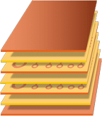
The inner layers have an oxide layer applied and then “stacked” together with pre-preg providing insulation between layers and copper foil is added to the top and bottom of the stack. The lamination process uses a combination of specific temperature, pressure for a specific time to allow the resin within the pre-preg to flow and bond the layers together to form a solid multilayer panel.
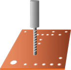
We now have to drill the holes that will subsequently create electrical connections within the multilayer PCB. This is a mechanical drilling process that must be optimized so that we can achieve registration to all of the inner layer connections. The panels can be stacked at this process. The drilling can also be done by a laser drill.
TCX ADDED VALUE
Each order undergoes first sample inspection before production.All equipment are inspected regularly.
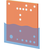
PTH provides a very thin deposit of copper that covers the hole wall and the complete panel. A complex chemical process that must be strictly controlled to allow a reliable deposit of copper to be plated even onto the non-metallic hole wall. Whilst not a sufficient amount of copper on its own, we now have electrical continuity between layers and through the holes.
TCX ADDED VALUE
The PTH production line is automatic.
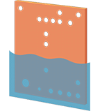
Panel plating follows on from PTH to provide a thicker deposit of copper on top of the PTH deposit – typically 5 to 8 um. The combination is used to optimize the amount of copper that is to be plated and etched in order to achieve the track and gap demands.
TCX ADDED VALUE
TCX produces through hole plating of minimum 20um as standard, which provides greater reliability of the via structure and improved z-axis expansion performance.
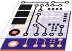
Similar to the inner layer process, but with one main difference – we will remove the dry film where we want to keep the copper/define circuitry – so we can plate additional copper later in the process.
This step of the process is performed in a clean room.
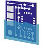
Second electrolytic plating stage, where the additional plating is deposited in areas without dry film (circuitry). Increases the plating thickness to meet demands including NCAB Group demands with and average of 25um / min 20um through the hole. Once the copper has been plated, tin is applied to protect the plated copper.
TCX ADDED VALUE
TCX provides through hole plating of 20um nominal as standard. This provides greater reliability of the via structure and improved z-axis expansion performance.

This is normally a three-step process. The first step is to remove the blue dry film. The second step is to etch away the exposed/unwanted copper whilst the tin deposit acts an etch resist protecting the copper we need. The third and final step is to chemically remove the tin deposit leaving the circuitry.
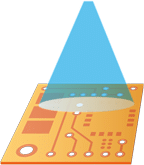
Just like with inner layer AOI the imaged and etched panel is scanned to make sure that the circuitry meets design and that it is free from defects. Again no repair of open circuits are allowed under TCX demands.
TCX ADDED VALUE
All PCBs are tested only by the approved equipment and no track welding or open circuit repair is allowed. This provides
increased reliability as there is no risk of repair failure, nor will this impair signal integrity.
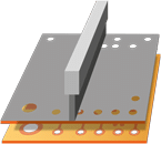
Using soldermask ink or epoxy resin and a prepared stencil, with holes in the stencil that align with the via holes we wish to plug, we use a screen printing process to push ink or resin into holes. Unlike soldermask we are trying to push ink through the holes in the PCB and judge quality based upon the IPC standard of ≥ 70% fill.
This step of the process is performed in a clean room.
TCX ADDED VALUE
With ≥ 70% soldermask fill on type VI via holes, TCX provides less risk of via holes causing rejection during assembly.
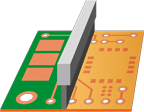
Soldermask ink is applied over the whole PCB surface. Using artworks and UV light we expose certain areas to the UV and those areas not exposed are removed during the chemical development process – typically the areas which are to be used as solderable surfaces. The remaining soldermask is then fully cured making it a resilient finish.
This step of the process is performed in a clean room.
TCX ADDED VALUE
TCX has proceed the standard of soldermask thickness with ≥ 5um on the knee of the track and between 10-30um on the surface.
TCX PCBs offer improved electrical insulation and an improved resilience to chemistry or mechanical force that could cause loss of soldermask.

Various finishes are then applied to the exposed copper areas. This is to enable protection of the surface and good solderability. The various finishes can include Electroless Nickel Immersion Gold, HASL, Immersion Silver etc. Thicknesses and solderability tests are always carried out.
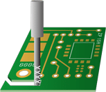
This is the process of cutting the manufacturing panels into specific sizes and shapes based upon the customer design as defined within the Gerber data. There are 3 main options available when providing the array or selling panel – scoring, routing or punching. All dimensions are measured against the customer supplied drawing to ensure the panel is dimensionally correct.
TCX ADDED VALUE
All equipment has clear operating instructions. Unless otherwise specified, default tolerances are applied to all designs.
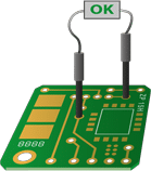
Used for checking the integrity of the tracks and the through hole interconnections – checking to ensure there are no open circuits or no short circuits on the finished board. There are two test methods, flying probe for smaller volumes and fixture based for volumes.
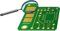
Visual checking the PCB against acceptance criteria. Using manual visual inspection and AVI – compares PCB to Gerber and has a faster checking speed that human eyes, but still requires human verification. All orders are also subjected to a full inspection including dimensional, solderability, etc.
TCX ADDED VALUE
Each PCB is inspected against the 100+ points as a standard requirement and every batch is subject to a full evaluation prior to shipment to ensure the PCBs are produced to the highest
standard.
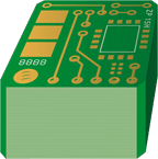
Boards are wrapped using materials that comply with the standard packaging demands (ESD etc.) and then boxed prior to be being shipped using the requested mode of transport.
