MULTILAYER
What is a multilayer PCB?
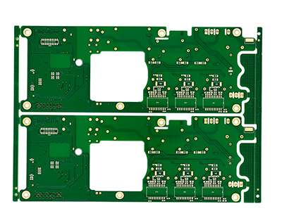
It is a PCB made with three or more conductive copper layers. The conductive foil appears to be various layers of a multi-sided circuit board. The different inner layers are processed in pairs (on a core) and then bonded together using prepreg as the insulating layer. The layers are then placed in such a way that both sides of the PCB can be used to mount components with additional tracking/electrical connections on the inside of the board. Vias are used as a source of the electrical connections between the different layers of a multilayer PCB.
Many products use multilayer PCBs, including computers, medical equipment, in-car systems, GPS and satellite systems, industrial control systems
Please contact us if you need further information or assistance, we are happy to help you.

PCB Manufacturing Capabilities | |||
Product feature | Standard | Advanced | |
Layer count | 32L | 40L | |
Board thickness | 5.5mm | 6.5mm | |
Aspect ratio | 10:1 | 14:1 | |
Copper thickness | 6OZ | 12OZ | |
2L | 500×1200mm | 540×1200mm | |
≥4L | 540*650mm | 540*650mm | |
Min. 4L board thickness | 0.38mm | 0.35mm | |
Min. hole & pad size | 0.20/0.40mm | 0.15/0.35mm | |
Drilling Accuracy | ±0.05mm | ±0.038mm | |
Min. solder mask bridge | 0.065mm | 0.065mm | |
PTH hole size tolerance | ±0.05mm | ±0.038mm | |
Contour tolerance | ±0.05mm | ±0.05mm | |
Impedance tolerance | ±8% | ±6%(Differential impedance) | |
Min. line width/spacing | 0.075/0.075mm | 0.065/0.065mm | |
Surface Treatment | HAL, LF HAL, ENIG, Immersion Silver, Immersion Tin, OSP, ENIPIG, Plating hard gold, Gold finger (contain segmented golden finger), ENIG+OSP, ENIG+gold finger, Immersion Tin+gold finger, Immersion Silver+gold finger | ||
