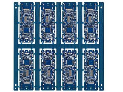
HDI
We pride ourselves on having a team of skilled engineers and technicians who are well versed in the intricacies of HDI PCB manufacturing. With years of experience behind us, we’ve mastered the art of creating intricate designs that push the boundaries of innovation.
What defines a HDI board?
IPC-2226 defines HDI as a printed circuit board with a higher wiring density per unit area than conventional printed circuit boards (PCB). There are different types of HDI features, type I, type II and type III as defined in IPC-2226. In our FAQ you can learn more about the different types.
Please contact us if you need further information or assistance, we are happy to help you.

HDI Manufacturing Capabilities | ||
Product feature | Standard | Advanced |
HDI stage | 3+N+3 | Anylayer |
Aspect ratio for blind via | 1:1 | 1:1 |
Min. 8L board thickness | 0.70mm | 0.65mm |
Min. line width/spacing | 0.05/0.05mm | 0.05/0.05mm |
Key line/tolerance | 0.065mm/15% | 0.06mm/10% |
Min. blind via diameter | 0.10mm | 0.09mm |
Min. capture pad size | 0.23mm | 0.20mm |
Min. PTH diameter | 0.20mm | 0.175mm |
Min. PTH PAD size | 0.35mm | 0.30mm |
Min. clearance(copper to SM opening) | 0.038mm | 0.025mm |
Min. solder mask bridge | 0.065mm | 0.065mm |
Min. CSP/BGA pitch | 0.40mm | 0.35mm |
PTH hole size tolerance | ±0.05mm | ±0.038mm |
Contour tolerance | ±0.05mm | ±0.05mm |
Impedance tolerance | ±8% | ±6%(for differential impedance) |
Surface Treatment | HAL, LF HAL, ENIG, Immersion Silver, Immersion Tin, OSP, ENIPIG, Plating hard gold, Gold finger (contain segmented golden finger), ENIG+OSP, ENIG+gold finger, Immersion Tin+gold finger, Immersion Silver+gold finger | |
